- 您现在的位置:买卖IC网 > Sheet目录1995 > HI5728/6INZ (Intersil)DAC DUAL 10-BIT 60MHZ 48-LQFP
18
FN4321.5
January 22, 2010
Voltage Reference
The internal voltage reference of the device has a nominal
value of +1.2V with a
±60 ppm/°C drift coefficient over the full
temperature range of the converter. It is recommended that a
0.1
μF capacitor be placed as close as possible to the REFIO
pin, connected to the analog ground. The REFLO pin (15)
selects the reference. The internal reference can be selected if
pin 15 is tied low (ground). If an external reference is desired,
then pin 15 should be tied high (to the analog supply voltage)
and the external reference driven into REFIO, pin 23. The full
scale output current of the converter is a function of the voltage
reference used and the value of RSET. IOUT should be within
the 2mA to 20mA range, through operation below 2mA is
possible, with performance degradation.
If the internal reference is used, VFSADJ will equal
approximately 1.16V (pin 22). If an external reference is used,
VFSADJ will equal the external reference. The calculation for
IOUT(Full Scale) is:
If the full scale output current is set to 20mA by using the
internal voltage reference (1.16V) and a 1.86k
Ω R
SET
resistor, then the input coding to output current will resemble
the following:
Outputs
IOUTA and IOUTB (or QOUTA and QOUTB) are
complementary current outputs. The sum of the two currents
is always equal to the full scale output current minus one
LSB. If single ended use is desired, a load resistor can be
used to convert the output current to a voltage. It is
recommended that the unused output be either grounded or
equally terminated. The voltage developed at the output
must not violate the output voltage compliance range of
-0.3V to 1.25V. RLOAD should be chosen so that the desired
output voltage is produced in conjunction with the output full
scale current, which is described above in the ‘Reference’
section. If a known line impedance is to be driven, then the
output load resistor should be chosen to match this
impedance. The output voltage equation is:
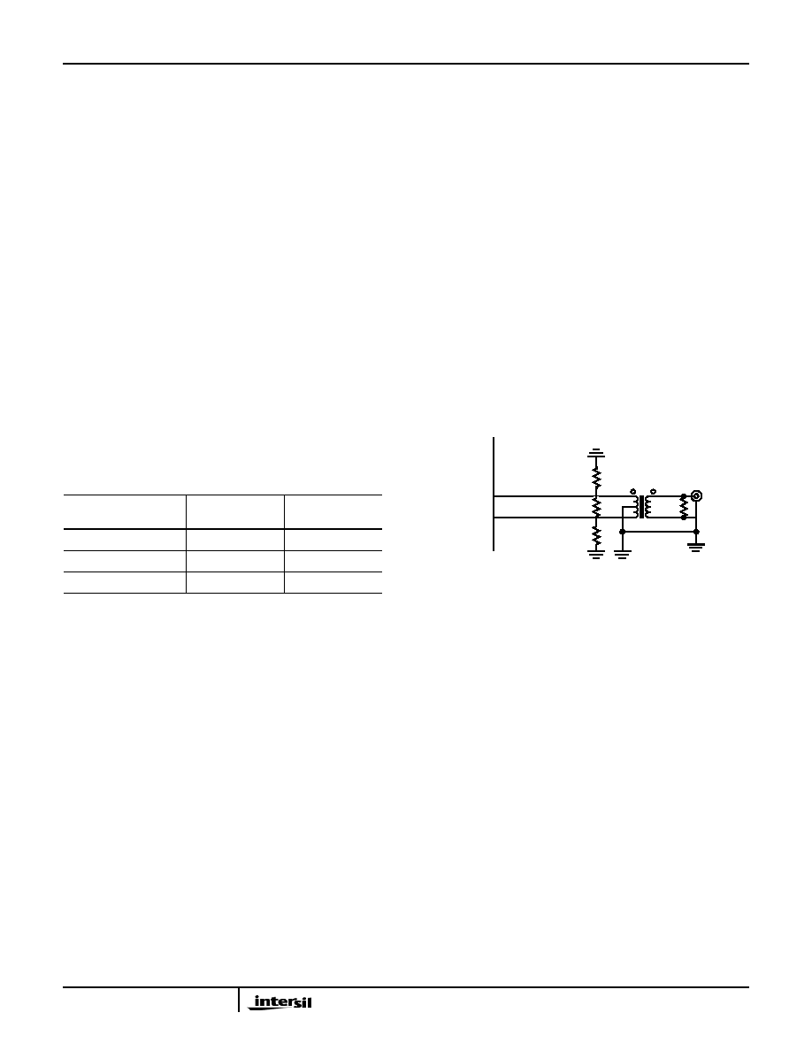
These outputs can be used in a differential-to-single-ended
arrangement to achieve better harmonic rejection. The
SFDR measurements in this data sheet were performed with
a 1:1 transformer on the output of the DAC (see Figure 1).
With the center tap grounded, the output swing of pins 16
and 17 will be biased at zero volts. It is important to note
here that the negative voltage output compliance range limit
is -300mV, imposing a maximum of 600mVP-P amplitude
with this configuration. The loading as shown in Figure 1 will
result in a 500mV signal at the output of the transformer if
the full scale output current of the DAC is set to 20mA.
VOUT = 2 x IOUT x REQ ,where REQ is ~12.5Ω.
Allowing the center tap to float will result in identical
transformer output, however the output pins of the DAC will
have positive DC offset. The 50
Ω load on the output of the
transformer represents the spectrum analyzer’s input
impedance.
TABLE 1. INPUT CODING vs OUTPUT CURRENT (Per DAC)
INPUT CODE (D9-D0)
IOUTA
(mA)
IOUTB
(mA)
11111 11111
20
0
10000 00000
10
00000 00000
0
20
I
OUT Full Scale
() V
FSADJ RSET
32
×
=
(EQ. 1)
V
OUT
I
OUT
R
LOAD
×
=
(EQ. 2)
PIN 17 (20)
PIN 16 (21)
VOUT = (2 x IOUT x REQ)V
100
Ω
50
Ω
50
Ω
50
Ω
IOUTB (QOUTB)
IOUTA (QOUTA)
FIGURE 42.
HI5728
发布紧急采购,3分钟左右您将得到回复。
相关PDF资料
HI5731BIBZ
DAC 12BIT 100MHZ 5.2V 28-SOIC
HI5735KCBZ
CONV D/A 12BIT 80MSPS 28-SOIC
HI5741BIBZ
DAC 14BIT 100MHZ 5.2V 28-SOIC
HI5746KCB-T
CONV A/D 10BIT 40MSPS 28-SOIC
HI5760BIBZ
CONV D/A 10-BIT 125MSPS 28-SOIC
HI5762/6IN
CONV A/DDUAL 10BIT 60MSPS 44MQFP
HI5766KCB
CONV A/D 10BIT 60MSPS 28-SOIC
HI5767/6IB
CONV A/D 10BIT 60MSPS 28-SOIC
相关代理商/技术参数
HI5728EVAL1
功能描述:数据转换 IC 开发工具 HI5728EVAL PLA TFORM FOR TQFP
RoHS:否 制造商:Texas Instruments 产品:Demonstration Kits 类型:ADC 工具用于评估:ADS130E08 接口类型:SPI 工作电源电压:- 6 V to + 6 V
HI5728EVALI
制造商:Rochester Electronics LLC 功能描述:- Bulk 制造商:Harris Corporation 功能描述:
HI5728IN
功能描述:DAC DUAL 10BIT 125MHZ 48-TQFP RoHS:否 类别:集成电路 (IC) >> 数据采集 - 数模转换器 系列:- 标准包装:2,400 系列:- 设置时间:- 位数:18 数据接口:串行 转换器数目:3 电压电源:模拟和数字 功率耗散(最大):- 工作温度:-40°C ~ 85°C 安装类型:表面贴装 封装/外壳:36-TFBGA 供应商设备封装:36-TFBGA 包装:带卷 (TR) 输出数目和类型:* 采样率(每秒):*
HI5728IN-T
功能描述:DAC DUAL 10BIT 125MHZ 48-TQFP RoHS:否 类别:集成电路 (IC) >> 数据采集 - 数模转换器 系列:- 标准包装:2,400 系列:- 设置时间:- 位数:18 数据接口:串行 转换器数目:3 电压电源:模拟和数字 功率耗散(最大):- 工作温度:-40°C ~ 85°C 安装类型:表面贴装 封装/外壳:36-TFBGA 供应商设备封装:36-TFBGA 包装:带卷 (TR) 输出数目和类型:* 采样率(每秒):*
HI5728INZ
功能描述:数模转换器- DAC W/ANNEAL 48 TQFP IND D/A 10BIT 125MHZ RoHS:否 制造商:Texas Instruments 转换器数量:1 DAC 输出端数量:1 转换速率:2 MSPs 分辨率:16 bit 接口类型:QSPI, SPI, Serial (3-Wire, Microwire) 稳定时间:1 us 最大工作温度:+ 85 C 安装风格:SMD/SMT 封装 / 箱体:SOIC-14 封装:Tube
HI5728INZ-T
功能描述:数模转换器- DAC W/ANNEAL 10 BIT DL DAC 125MSPS 48 LQFP RoHS:否 制造商:Texas Instruments 转换器数量:1 DAC 输出端数量:1 转换速率:2 MSPs 分辨率:16 bit 接口类型:QSPI, SPI, Serial (3-Wire, Microwire) 稳定时间:1 us 最大工作温度:+ 85 C 安装风格:SMD/SMT 封装 / 箱体:SOIC-14 封装:Tube
HI5731
制造商:INTERSIL 制造商全称:Intersil Corporation 功能描述:12-Bit, 100MSPS, High Speed D/A Converter
HI5731_04
制造商:INTERSIL 制造商全称:Intersil Corporation 功能描述:12-Bit, 100MSPS, High Speed D/A Converter